Original article: CUI.COM – EMI Filter Components
As your project progresses, you have reached a critical juncture where you must choose the appropriate internal AC-DC and DC-DC power supplies. In your previous project, you opted for supplies with internal EMI and EMC components. However, the current project requires external EMI and EMC components for the supplies you are evaluating. In this discussion, we will guide you through the reasons behind this requirement and how to select the appropriate components.
Before delving into the specifics of EMI and EMC components selection, let’s clarify their fundamental concepts. EMI and EMC are acronyms that stand for Electromagnetic Interference and Electromagnetic Compatibility, respectively. Essentially, these concepts boil down to two primary goals: avoiding disruption to other systems and functioning correctly in the presence of external electrical disturbances.
Now, let’s dive into the nitty-gritty of EMI and EMC component selection. Our focus will be on external components since your current project demands their use. First and foremost, it’s essential to understand that the selection of EMI and EMC components is not one-size-fits-all. The components required will vary depending on factors such as the project’s electromagnetic environment and the specific power supply being used. Therefore, it’s crucial to consult with a knowledgeable engineer or supplier to determine the appropriate components.
It’s also important to note that selecting the wrong EMI or EMC components can result in poor system performance, leading to increased cost and delayed project timelines. Therefore, it’s crucial to invest time and resources in proper component selection to ensure optimal system performance.
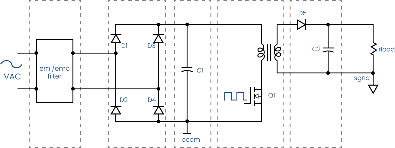
Fig. 1 – Simplified block diagram of ac-dc switching power supply
While the diagram simplifies the EMI/EMC filter as a single block at the power supply’s input, real-world applications get more strategic. These essential components are distributed across the input, output, and even internally within the power supply.
Think of them as a multi-layered defense system: they tackle unwanted electrical noise both entering and exiting the supply, act as a shield against sudden voltage spikes, control that initial surge of power when the supply is turned on, and even act as a safety net for the power source itself in case of a power supply failure.
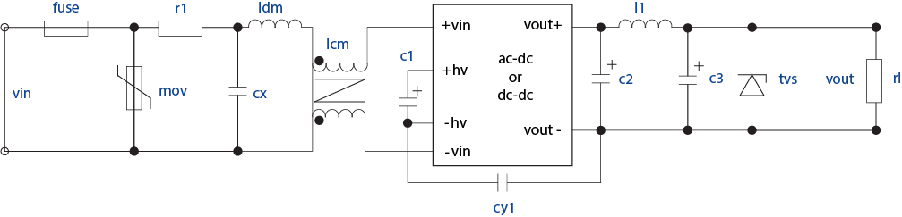
Fig.2 – External EMI and EMC components
The fuse acts as the first line of defense, standing guard between the power source and the power supply itself. Its critical job is to sever the connection if the current surges too high, preventing damage to both the power source and its wiring.
To ensure maximum protection, the fuse is directly connected to the power source, with no other components in between.It’s strategically placed in series with the non-ground input terminal, so that if it blows, the entire power supply is de-energized.
Remember, a blown fuse is a red flag. It signals a potential problem within the power supply, not just a simple overload.So, instead of just replacing the fuse and hoping for the best, it’s crucial to investigate and repair or replace the power supply itself.
Choosing the right fuse is about more than just its current rating. Factors like voltage, response time, operating temperature, and even its physical package all need to be considered to ensure optimal performance and protection.
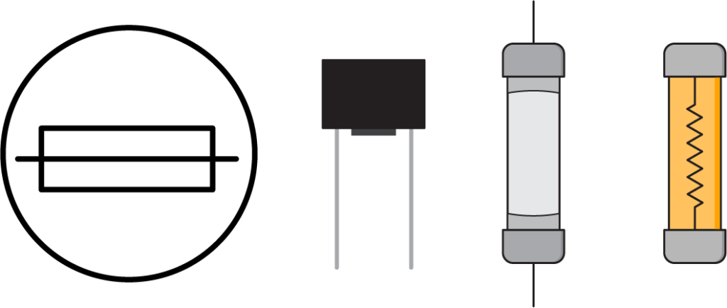
Fig. 3 – Fuse symbol (left) and mounting styles (right)
The Metal Oxide Varistor (MOV), strategically placed across the input terminals, acts like a safety valve for voltage spikes. When the AC power lines experience a surge, whether from a lightning strike or some other disruption, the MOV kicks in. It’s normally high-impedance, blending into the background during regular operation, but when voltage surges above its rating, it becomes a low-impedance path, channeling the excess energy away from sensitive components.
Crucially, an input fuse always sits between the MOV and the power source. This fuse acts as a fail-safe, in case the MOV takes a hit that’s too big and its low-impedance state causes excessive current flow.
Selecting the right MOV requires careful consideration of both the normal operating voltage and the potential transient energy the power supply might encounter. While MOVs are a common choice, designers have other tools in their arsenal, such as Zener diodes, TVS diodes, or Gas Discharge Tubes (GDTs), each with its own strengths and tradeoffs.
Resistor R1 is the gatekeeper, controlling the initial rush of current when an AC-DC power supply is switched on. Without it, the bulk capacitor would charge up like a thirsty traveler at an oasis, creating a surge potentially a hundred times greater than normal operating levels.
While a higher resistance value reins in this surge, it also creates a drag on the system during normal operation. The resistor’s construction is key: it needs to be tough enough to withstand that initial energy burst. Wire wound resistors, known for their robust build, are a common choice. Film resistors, however, are typically not up to the task.
Fig, 4 – Input Surge Current Limiting Resistor
Some designs employ a clever trick: a negative temperature coefficient (NTC) resistor. It starts off with high resistance, acting as a dam to the initial surge of current. But as current flows and heats it up, its resistance decreases, allowing a smooth flow of power.
Think of it like a smart bottleneck that widens as needed. However, once the power supply is off, the NTC needs time to cool down and ‘reset’ its high resistance. So, give it a few moments before turning things back on.
Interestingly, many DC-DC converters don’t even need a dedicated surge-limiting resistor. Their design, combined with factors like low input voltage or the nature of the power source, might already keep surges under control.
The TVS diode, stationed at the power supply’s output, wears two hats. Firstly, it acts as a lightning rod for voltage surges, channeling any externally-induced transients safely away to protect the power supply itself. While MOVs handle similar duties on the input side, TVS diodes are the better choice for the output due to typically lower voltages and transient energies.
Secondly, the TVS can be swapped for a Zener diode if there’s a need to cap the output voltage should the power supply fail. However, be warned: the Zener may need to handle power exceeding the supply’s rated output, as a failing supply could potentially deliver more than its normal current.
Inductor LDM, working in conjunction with input capacitor CX, forms a noise-filtering tag team on the power supply’s input. It effectively blocks unwanted conducted noise, preventing it from flowing back and polluting the external power source.
When selecting LDM, its saturation current is crucial. It must be able to comfortably handle the maximum current during normal operation, even if it briefly saturates during the initial power-up surge. Additionally, its parasitic DC resistance should be low enough to avoid wasting power as heat.
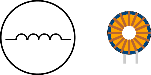
Fig. 5 – Differential Mode Choke
The LCM choke with dual windings functions as an input common mode choke, meaning it creates a high impedance to weaken common mode currents in the input conductors. While incorporating the common mode choke in the schematic, it’s crucial to ensure that the ‘dots’ are correctly oriented. These ‘dots’ indicate the relative winding direction for the pair of windings, and it doesn’t matter if they are on the input or output of the connections to the common mode choke. However, both dots must be on the same electrical side of the choke. Unlike the differential mode choke, the common mode choke does not require dot notation as it has only one winding, and the current flow direction does not matter.
It’s imperative to choose a common mode choke that can handle the maximum current flow during normal power supply operation while maintaining acceptable power dissipation. Usually, the common mode choke has minimal current flowing in common mode, making the saturation current rating insignificant.
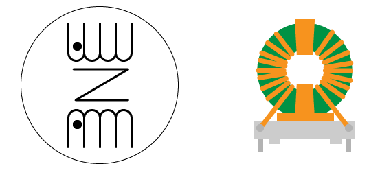
Fig. 6 – Common Mode Choke
The CX capacitor, placed across the input power lines, plays a crucial role in shunting the differential conducted voltage noise to prevent it from reaching the external voltage source. To ensure optimum performance, it is advisable to use a capacitor that belongs to the X or Y safety class construction. Such capacitors are designed to be directly connected to the AC input lines, making them capable of withstanding any voltage surges that may be present.
To better shunt the undesired noise, a larger value of capacitance is preferred as it results in a lower impedance. However, this also increases the input leakage current in an AC-DC power supply. It is essential to note that many AC-powered systems need to comply with regulatory standards that impose maximum input leakage current limits. Consequently, the amount of capacitance in the shunt capacitor is restricted.
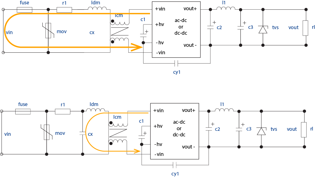
Fig. 7 – EMI current path with (top) and without (bottom) X-Capacitor
In the schematic diagram, there is a capacitor labeled CY1 that is placed between the input and output of the power supply to reduce common mode voltage noise on the output. This capacitor is selected to be of Safety Class Y since it is located across the isolation barrier. Safety Class Y capacitors are designed to fail in an open circuit, ensuring the integrity of the input to output isolation of the power supply in case of capacitor failure. Sometimes, two capacitors are required to be connected in series to provide further assurance of the isolation between the input and output of the power supply.
The need for capacitor CY1 arises due to the voltage waveform created by the primary side switching transistor, and the parasitic capacitance between the primary and secondary side of the isolation magnetics (as shown in Figure 8). To maximize its effectiveness, capacitor CY1 should be placed between the source of the primary side switching FET and the terminals of the secondary winding of the isolation magnetics. Additionally, since the output terminals of the isolation magnetics have large bypass capacitors between them, they are at the same AC potential. Therefore, the output terminal of capacitor CY1 can be connected to either output terminal.
The capacitance value of CY1 must be larger than the primary to secondary parasitic capacitance to ensure proper attenuation of the common mode voltage on the output of the power supply. However, it’s essential to note that a larger value of capacitor CY1 can cause greater AC leakage current between the input and output of the power supply.
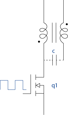
Fig. 8 – Primary Side Switch, Isolation Magnetics, and Parasitic Capacitance
Positioned strategically at the entrance to the DC-DC converter, capacitor C1 acts as a crucial buffer. It stabilizes input voltage fluctuations caused by sudden changes in current demand. In AC-DC supplies, C1 plays a dual role: smoothing out the pulsating DC voltage from the rectifier and providing a reserve of energy to maintain output voltage even when the AC input drops out.
Remember that input surge current limiting resistor we talked about? It’s there to control the initial rush of current when this capacitor is first charged.
The power supply’s output terminals can have filter components installed to tackle any EMI and EMC problems that may arise. Typically, these components are placed near the load and are chosen based on their ability to reduce the output ripple voltage to a level that the load can tolerate. In some cases, for ease of use, L1 may be substituted with a short circuit. It is important to note that capacitor C2 offers a low impedance ac pathway between the output terminals of the power supply, allowing CY1 to be linked to either output terminal.
To address EMI and EMC issues that may arise, filter components can be placed on the output terminals of a power supply. These components are usually positioned near the load and selected based on their ability to reduce output ripple voltage to a level that meets the load’s requirements. In certain situations, L1 can be replaced with a short circuit to simplify the process. It should be noted that capacitor C2 provides a low impedance ac pathway between the power supply’s output terminals, enabling CY1 to be linked to either terminal.
If you want to maintain the quality of your power supply, you should consider the installation of filter components on its output terminals. These components can be positioned near the load to ensure optimal reduction of output ripple voltage. In some cases, L1 may be substituted with a short circuit for convenience. Capacitor C2 is crucial in providing a low impedance ac pathway between the output terminals, which allows for CY1 to be linked to either terminal.
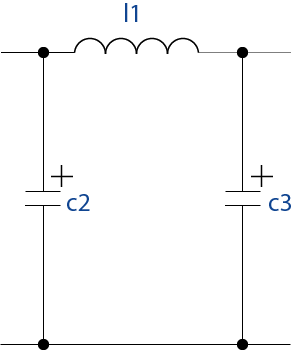
Fig. 9 – Output Filter
It is evident that choosing the appropriate components to avoid electromagnetic interference (EMI) and electromagnetic compatibility (EMC) problems related to power supplies is not a challenging task. However, it involves taking into account numerous factors. The ultimate decision regarding the components and their values is frequently a trade-off between performance, expense, size, and energy conversion efficiency.
Many power supply providers, including ALEXANDER ELECTRIC, have customer support engineers who are ready to offer further aid if needed during the implementation of your project. These professionals possess the expertise and knowledge to assist you in selecting the optimal components for your application, while also considering your project’s specific requirements and constraints.
In conclusion, while choosing the right components for your power supply might appear to be a simple task, it necessitates careful consideration of several factors. If you require additional support, do not hesitate to reach out to customer support engineers from reputable power supply manufacturers such as ALEXANDER ELECTRIC.

