 en
▼
en
▼
Gallium Nitride (GaN), a wide band-gap semiconductor material, is transforming the landscape of power supplies. In comparison to traditional silicon, GaN offers a promising avenue for manufacturers to enhance efficiency, reduce size, and decrease weight in power supply devices. This article explores the distinctive properties of GaN that enable these advancements.
Power transistors play a crucial role in contributing to power loss within a switching power supply. The losses associated with these transistors are typically categorized into two main types: conduction losses and switching losses. Conduction losses occur during the on state of the transistor, and switching losses happen during the transition between on and off states.
When GaN transistors are in the on state, they exhibit a resistance between the drain and source, commonly referred to as Ron. The conduction losses are directly proportional to this resistance. GaN, along with other Wide Bandgap (WBG) materials, offers a distinct advantage in the relationship between breakdown voltage and Ron. A comparison of silicon, GaN, and silicon carbide (SiC) in Figure 1 illustrates that, for a given breakdown voltage, the Ron of WBG devices, especially GaN, is significantly lower than that of silicon. As silicon approaches its theoretical limit, the adoption of GaN and other WBG materials becomes imperative for continued improvements in Ron.
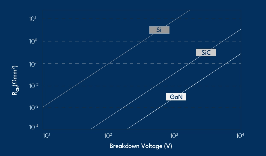
Fig.1 – Theoretical limits of Ron vs. breakdown voltage for Si, GaN, and SiC transistors
Beyond enhancements in conduction losses, the utilization of GaN also contributes to a reduction in switching losses. Various factors contribute to switching losses, many of which GaN helps improve. One such mechanism involves the current in a transistor starting to flow before the drain-source voltage begins to fall, resulting in substantial losses during this transition, as depicted in Figure 2. GaN’s faster switching speed compared to silicon enables a reduction in losses during this transition.
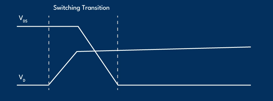
Fig.2 – Drain Voltage and current waveforms during switching transition
Another way GaN minimizes switching losses is by eliminating the need for a body diode. During the “dead-time” when both switches of a half-bridge are off to prevent a short circuit, current continues to flow. In silicon transistors, this current is forced through the less efficient body diode, leading to increased losses. However, GaN transistors lack a body diode, directing the current through the Ron resistance instead. This substantially decreases the losses incurred during the dead-time.
Moreover, the absence of a body diode in GaN transistors eliminates nearly all reverse recovery losses, a phenomenon where the body diode conducts during the dead-time and must be turned off when the other switch activates. This results in additional losses due to reverse current flow. GaN’s design mitigates these losses, making it a more efficient choice in power supply applications.
Switching losses, when averaged over time, benefit from GaN’s lower losses, allowing for a higher switching frequency. The increased frequency facilitates a reduction in the size of key components, such as transformers, inductors, and output capacitors. Additionally, GaN devices boast better thermal conductivity and higher temperature resistance than silicon, reducing the need for bulky thermal management components like heatsinks and fans. These factors collectively contribute to a significant decrease in the overall size of power supplies.
A tangible application of GaN’s benefits can be observed in Alexander Electric’s latest series of power supplies.
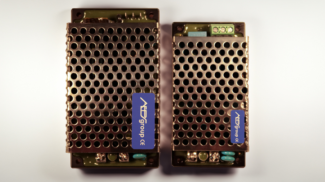
Fig.3 – Comparison of Si based and GaN based power unit form factors
The increased switching frequency of the JETA100-LP has led to a remarkable size reduction of 20%, accompanied by a 25% weight reduction. The power density has surged from 17 W/in3 to 21 W/in3, showcasing the transformative impact of GaN technology. These AC/DC power units, leveraging GaN, achieve efficiencies up to 96%, marking a substantial leap from conventional silicon-based supplies.
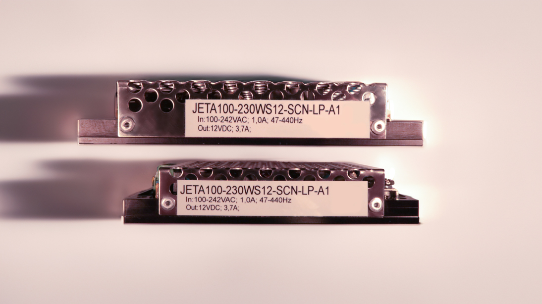
Fig.4 – Comparison of Si based and GaN based power unit form factors (2)
As silicon approaches its physical limits, GaN emerges as a pivotal player in the quest for enhanced power supply efficiency and reduced form factor. Manufacturers, exemplified by Alxander Electric’s latest generation of GaN-based adapters, are leveraging GaN’s unique properties to design smaller, more efficient power supplies. GaN’s journey continues to unfold, promising ongoing improvements and innovations in the realm of power electronics.
