In the “first and second” grades we considered some basics of construction of a very important circuit for power electronics – a single forward converter (FC).
It should be noted at once – small mistakes when considering very big and important issues sometimes happen. That’s why the captions under figures 6 and 7 (“first grade”) should be quite different – “Diagrams of currents and voltages in FC elements with a choke continuous current” and “Diagrams of currents and voltages in FC elements with a choke discontinuous current” respectively.
Yes, and the reasoning is tortured – what is the right single or single? The fact is that the author has prepared for further consideration (check for the further articles) interesting circuits built on a combination of two converters. And if they will be “double” converters – then the term “single” is convenient, but most likely the author will settle on the term “twin” – and of course it is more correct – “single”. Same letter, but more fun. Agree, “single” is something too sad for such a wonderful and important device.
So, having considered the scheme of forward converter (FC), and giving it the title “Mercedes among DC/DC converters” for high power efficiency, let’s try to find something opposite, conceptually different – a kind of “Peugeot” (or “Toyota” for someone like…) among electric power supply sources. Such “Peugeot” is the most widespread in the world practice flyback converter.
Recall how the ignition coil in a car works. First, the primary winding of the ignition coil is connected to the battery through the breaker contacts with a shunt (interference suppression) capacity, and then, after opening the contacts, the energy stored in the coil and “jumped” into the secondary winding is discharged to the spark plug, in which an arc discharge occurs, by the way, stabilizing the voltage! That’s when in the olden days this was invented, that’s when the first SPSs appeared – flyback converters.
So – what is this “Peugeot” among SPSs?
A schematic of such a converter is shown in Figure 1. The elements are highlighted in blue and their action will be explained in a further, closer look at the flyback converter.
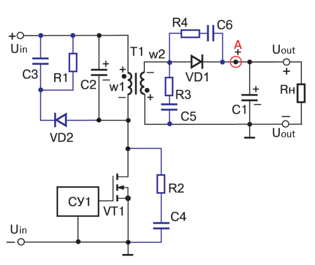
Fig. 1 – Schematic of the power section of a flyback converter
The input supply voltage U is connected to the primary winding w1 of transformer T1 in series and a switch realized on transistor VT1. Let’s assume that the MOSFET switch is ideal, it switches quickly (conditionally – instantly) from on to off and vice versa, and the voltage drop on the on MOSFET is vanishingly small. The Uin source is stabilized, and the high-frequency pulse currents of the converter are easily short-circuited through it. The capacitor C2 is (to some approximation) the equivalent capacitance of all capacitances given to the primary winding w1 of transformer T1:
etc., up to the capacitance intentionally supplied by the designer of the SPS. For both forward converter and flyback converter, the capacitance of C2 always exists, and for high-frequency transducers it cannot be neglected.
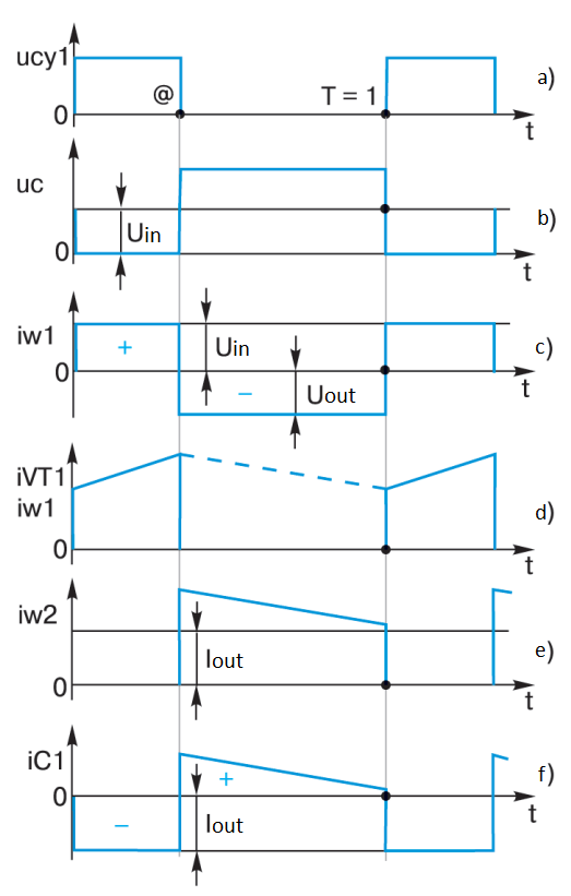
Fig.1 – Voltage and current diagrams in the flyback converter circuit for the continuous current mode
The control circuit of IC1 delivers control pulses to the gate of MOSFET VT1 (see Fig. 2a), which are sufficient to reliably open transistor VT1. With a pulse repetition period T, the relative duration of each pulse is @. With transistor VT1 open, the primary winding w1 of transformer T1 is connected to the input voltage source Uin. The ideal oscillogram at the transistor drain is shown in Figure 2b. For a time @ there is a constant voltage Uin (see Figure 2 c) on the winding wl and capacitor C2.The initial voltage polarity on the transformer windings and on capacitor C2 is shown in Figure 1.
On the secondary winding w2 of transformer T1 there is a voltage of the same shape and magnitude according to the transformer ratio for a time @. Up to the time @ the output diode VD1 is closed by the negative voltage coming from winding w2.
According to the formula for inductance, the current through the inductance of winding w1 (through transistor VT1) increases linearly for time @ (see Fig. 2d). Since there is no energy transfer to the load (the output diode is closed), energy W = L1 * I2/2 is stored in the winding inductance w1.
When transistor VT1 is turned off at time @, the turn off and current drop through transistor VT1 is “instantaneous”. Conditionally instantaneously (correctly, very quickly) capacitor C2 is discharged to zero, because at that point in time it gives off a large operating current to winding w1 (i.e., it briefly acts as a source of input voltage). But since the current in the inductance cannot disappear instantly, it almost instantly recharges capacitor C2 in the opposite polarity to that shown in Figure 1 to a voltage of Uout . At the same time due to the appearance of a voltage on the winding w2 with polarity opposite to that shown in Figure 1, the diode VD1 opens instantly. As a result winding w2 through diode VD1 is connected to capacitor C1, i.e. to the load.
Here it is important to assume that the capacitance of capacitor C1 is large enough to neglect the voltage ripple on it, so the voltage on the load is stable and constant.
Since the energy stored in w1 practically has not been spent anywhere (of course, we take into account that in the capacitor C2 there is stored energy W = C2 * Uout2/2), from the moment of time @ it is spent for charging of the capacitor C1 and for loading power (see Fig. 2 e) in the form of falling current of the winding w2.
It should be noted, dear reader, that Peugeot, i.e., this flzback converter, is not a piece of cake. It hides an intrigue even in these simple processes. Look carefully at Figure 2. Naturally, while the current through winding w2 will exist the whole interval from time @ to 1 (i.e. to T), winding w2 will actually be connected to the DC output voltage through open diode VD1. This is what forms the rectangular portion of the voltage on winding wl of magnitude Uout . But since the volt-second area of the voltage on the inductance over a period is always zero (see Fig. 2c), then knowing the input supply voltage and the open time of the switch VT1, the reader will always could calculate the output voltage of the flyback converter in an elementary way. By the way, quite without the complicated conclusions given in textbooks: Uout = Uin * N * @ / (1 – @), where N = w2/w1 of the transformation of T1.
The regulating characteristic (and this expression is it) of the flyback converter, unlike that of the forward converter, is non-linear. Here the pleasant surprise is that it is simple and easy to derive graphically.
But for the current through capacitor C1, given that the ampere-second area per period for the capacitor is always zero (see Fig. 2 e), it is easy to see that if the top of the current pulse has a steep enough slope in the interval from @ to 1 (T), then at the end of this interval the current given by capacitor C1 (negative current values) will necessarily not be rectangular in shape, as it is often drawn in textbooks, but with a characteristic gentle descending segment. These two interesting surprise moments were shown by the author in Figures 3 and 4.
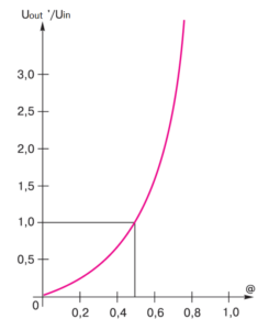
Fig. 3 – Regulating characteristic of the flyback converter
The regulating characteristic of the flyback converter (see Fig. 3), in addition to the fact that it is nonlinear, also indicates that in the flyback converter the same changes @, as in the forward converter, lead to large changes in the output voltage. That is, the flyback converter is regulated over a wider range. In practice, an @ range of 0 to 0.7 (maximum) is used. But the part of Figure 2 diagram in Figure 4 clearly reveals the aforementioned declining section of current through capacitor C1.

Fig. 4 – Current diagrams in the flyback converter circuit for discontinuous currents mode
The mode in which the winding current w2 does not have time to decay to zero during the time from @ to 1 (T) is the discontinuous current mode. Naturally, there can also be a discontinuous current mode (see Fig. 5).
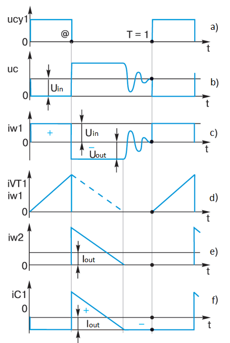
Fig. 5 – Diagrams of currents and voltages in the flyback converter circuit for discontinuous currents mode
Here there is an interesting feature – the secondary winding current after some time from the moment @ becomes equal to 0 – i.e. all the energy stored in the transformer T1 during the open time of the power transistor VT1 passes into the output capacitance C1 and the load. As a result, the voltage on winding w2 at this point could be zero (if there is no change in current in the inductance, there is no voltage), but we have forgotten about capacitance C2.
The energy accumulated in it W = C2 * Uout2/2 from this moment of time causes an oscillatory process (see Fig. 5 b and c), and free because w1 is free – the power transistor VT1 is off, and w2 is free – the diode VD1 is closed. In fact, there is still a small loss in C2 in our circuit, which makes the aforementioned oscillatory process damped.
What is characteristic for the discontinuous current mode? It is easy to see that the volt-second area on the interval from @ to 1 (T) has changed fundamentally. Since the working part of the pulse at this interval has decreased, transformer T1 compensates for the volt-second area by increasing the voltage Uout, if we leave the volt-second pulse area for the time from 0 to @ unchanged, as in the discontinuous currents mode. That is, the flyback converter in discontinuous current mode starts overestimating the output voltage!
You see how many subtleties arise in the operation of even an ideal flyback converter circuit, in this seemingly simple “Peugeot”! Here you have the need to assume losses in an initially lossless circuit and a rather interesting additional mode at continuous currents on the interval from @ to 1 (T).
Who conducts all these absurdities, is there a peculiar “lord of the rings”, such as io in forward converter? Yes – it is the inductance of transformer windings (it is enough to operate with the value of one inductance, for example, L1 of the primary winding wl , as the others are rigidly connected with it through transformation ratios. For example, for winding w2: L2 = L1 x N2).
Indeed, as we have shown, many processes in the flyback converter change their quality depending on the rate of rise and fall of the operating currents in the T1 windings. Let’s try to derive the ratio for the load current boundary mode (boundary mode because it separates the mode of continuous currents and the mode of discontinuous currents in the T1 transformer windings).
Before proving it, let us note two peculiarities. The first is that the load current is the average of the winding current w2. Indeed, the load current is a direct current. No direct current can flow through the capacitor, and the only source of energy precisely for direct current at the output of the flyback converter is winding w2. So, it is sufficient to take the area of the current diagram w2 (see Fig. 2e) and divide it by the period T to obtain the load current Iout.
The second important feature of flyback converter is that the rate of change (decay) of winding current w2 at a constant output voltage and a constant inductance L2 is constant: di/dt = -Uout/L2. The inquisitive reader will easily deduce this from the formula for inductance. Therefore, with a given L1, and hence L2 = L1 * N2, we can imagine how we decrease the load current Iv and the winding current diagram w2 in this case, without changing the slope of the current pulse peak, decreases in height until it touches the rightmost point of the pulse peak slope on the ordinate axis.
In this case the boundary mode will occur, which divides the mode of continuous and discontinuous currents. Then
Δi / (T (1 – @min)) = Uout / L2
or
L1 = Uout * T * (1 – @min) / N2 * Δi;
but at the same time, defining the output current as the average of the current w2 gives the expression:
Iout = Δi * (1 – @min) / 2
or
Δi = 2Iout / (1 – @min).
The result is:
L1 = Uout * T * (1 – @min) / (2Iout * N2).
From this expression you can see that the smaller the load current, the greater the inductance of the transformer you need to provide. Remember how we drew a similar conclusion for the inductance of the forward converter output choke.
In the same way as for a forward converter, for a flyback converter with Iout = 0 the value of L1 = ∞, i.e. such a transformer will have to be wound “very, very long” and the only way to preserve the mode of continuous currents at low load currents is an additional “overload” of the flyback converter.
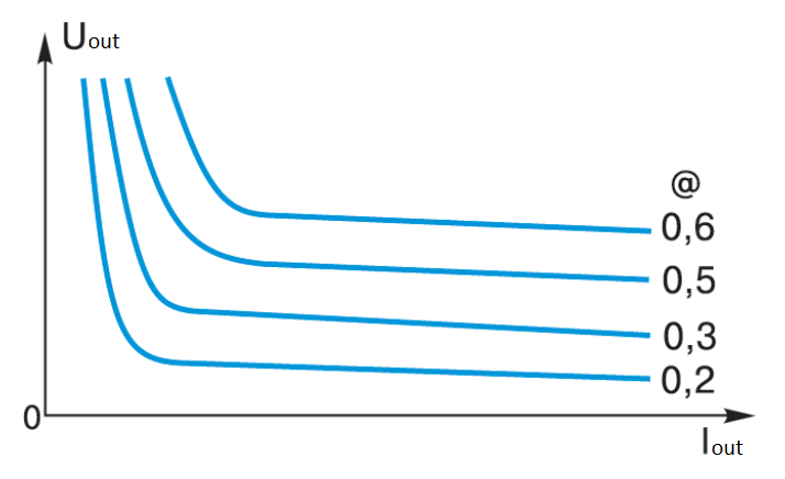
Fig. 6 – Regulatory characteristics of the flyback converter
The characteristic of the output voltage, depending on the presence of continuous and discontinuous currents, which the author gave for the description of the forward converter (“first grade”) is qualitatively relevant for the flyback converter as well (see Fig. 6). Such a characteristic shows the effect of “cocking” the output voltage when the load current decreases due to the discontinuous current mode L1 of transformer T1. But, as noted above, the discontinuous current mode in flyback converter can be very useful in the construction of high-voltage converters.
The most difficult thing in the flyback converter is the implementation of the transformer.
In essence, it is a multi-winding choke. Indeed, on the interval from 0 to @ the current in the winding w1 flows from its beginning to the end, forming a positive magnetic field strength of the transformer magnetic core T1, and on the interval from @ to 1 (T) the current in the winding w2 also flows from its beginning to the end and the sign of the magnetic field strength in the magnetic core does not change.
Thus, the magnetic coil of transformer T1 (now the choke) is under the action of the unidirectional magnetic field and is permanently magnetized. It is known that in this case special cores with a non-magnetic gap are used, for example ferrite cores made of two halves with a gap in the form of a non-magnetic pad. Usually it is this gap (after selecting the core) that generates the required inductance of the T1 windings.
Pressed magnetic cores are also widely used, e.g. MO-permalloy. This type of core is a grain of permalloy, pressed into the magnetic core with a non-magnetic binder. Multiple micro-gaps result in a uniformly distributed gap.
In this part of our lesson, it is useful to draw the reader’s attention to the positive role that capacitance C2 plays in the discontinuous current regime. When capacitance C2 discharges – forming a free oscillating process – the discharge current of capacitance C2 flows in the direction from the end of winding w1 to its beginning. This leads to the effect of a certain demagnetization of the magnetic core of transformer T1.
Here the author assumes that by this point the readers are certainly tired, although they are already third graders. Therefore, other interesting properties of flyback converter are in the next story – “grade”.

